
Publication in Nanoscale
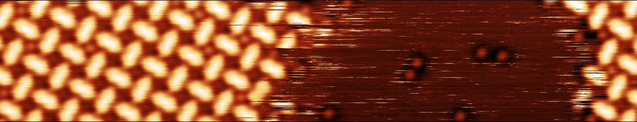
Our research on electron beam induced graphene doping was publidshed in nanoscale. We show thar full scale p- and n-doping can be achieved by lo energy electron beam irradiation at a specific gate voltage.
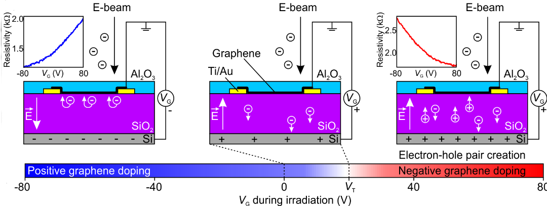
Schematic representation of the electric field within the device and its effect on the motion of electrons and holes within the device. For negative energies electrons entering the gate dielectrics are repelled away, for low positive voltages these electrons can drift through but do not possess enough energy to create electron-hole pairs. For the VG > VT electrons can in the electric field receive enough energy to induce formation of electron-hole pairs. The resulting doping is shown near the schematics.
See the paper here.