
Graphene as an Active Substrate
Graphene, a zero-bandgap semiconductor, attracted much interest for its mechanical, optical, and electronic properties. From our point of view, the most exciting feature is the possibility of controlling its electronic properties, i.e., the type of charge carriers and their concentration, by the external electric field.
Obtaining gated graphene devices working in UHV is challenging due to residues from lithographic processing on the graphene substrate. To circumvent the need for lithography, we have developed contactless methods to dope graphene employing X-rays or low-energy electrons. The irradiation-induced charge trapped in the dielectric layer acts the same way as a gate electrode and can provide higher doping than the standard way.
Another challenge is to prepare 2D metal-organic frameworks on a graphene substrate. We have developed a synthetic methodology to incorporate transition metal atoms and TCNQ molecules into the network on a graphene substrate.
Metal-Organic Frameworks on Graphene

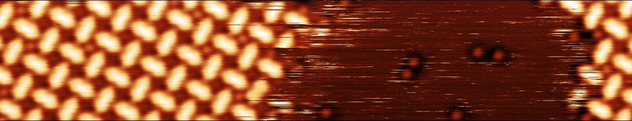
We have successfully synthesized metal-organic frameworks (MOFs) M-TCNQ (M = Ni, Fe, Mn) on epitaxial graphene/Ir(111), showing a single phase with M 1(TCNQ)1 stoichiometry. We demonstrate a remarkable chemical and thermal stability of TCNQ-based 2D MOFs: all the studied systems survive exposure to ambient conditions, with Ni-TCNQ doing so without any significant changes to its atomic-scale structure or chemical state. Thermally, the most stable system is Fe-TCNQ which remains stable above 500 °C, while all the tested MOFs survive heating to 250 °C. Overall, the modular M-TCNQ/graphene system combines the atomic-scale definition required for fundamental studies with the robustness and stability needed for applications; thus, we consider it an ideal model for research in single-atom catalysis, spintronics, or high-density storage media.
Z. Jakub et al.
: Remarkably stable metal-organic frameworks on an inert substrate: M-TCNQ on graphene (M = Mn, Fe, Ni).
Nanoscale 14 (2022), 9507.
Electron Beam Doping
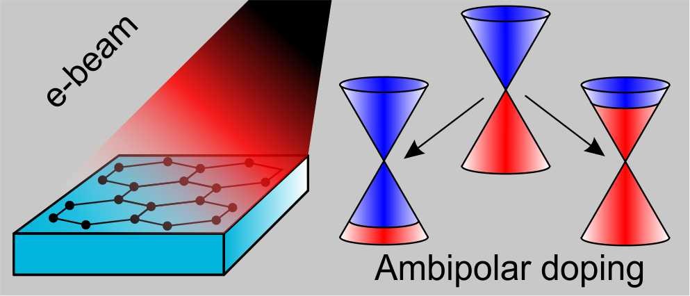
We employ the low energy electron beam irradiation to induce both n- and p-doping in the graphene layer. The type of dominant charge carriers induced in the graphene depends on the applied gate voltage. Irradiation of the graphene layer at the gate voltages higher (lower) than a specific threshold voltage VT value results in negative (positive) graphene doping. By designing the irradiation protocol a desired CNP position can be set.
V. Stará, P. Procházka, D. Mareček, T. Šikola, J. Čechal: Nanoscale 10, (2018), 17520.
X-Ray Doping

We have shown that the X-ray irradiation at the zero applied gate voltage causes very strong negative doping of graphene, which is explained by X-ray radiation induced charging of defects in the gate dielectric. The induced charge can be neutralized and compensated if the graphene device is irradiated by X-rays at a negative gate voltage: the charge neutrality point shifts back to zero voltage.
P. Procházka, D. Mareček, Z. Lišková, J. Čechal, T. Šikola, Sci. Rep. 7 (2017), 563.